The MIPS R8000 Microprocessor Chip Set from MIPS Technologies
implements a super-scalar architecture, providing supercomputer
performance at a fraction of the cost. The 64 bit architecture of the
MIPS R8000 Microprocessor is implemented using separate integer and
floating point devices. The impressive floating point performance of the
R8000 Microprocessor Chip Set makes it ideal for applications such as
engineering workstations, scientific computing, 3-D graphics
workstations, and multi-user systems. The high throughput is achieved
through complete separation of the integer and floating point functions,
the use of wide, dedicated data paths, and large on- and off- chip
caches.
The R8000 Microprocessor Chip Set implements the MIPS IV instruction
set. MIPS IV is a superset of the MIPS III instruction set and is
backward compatible. Implementing a 3.3 volt technology with a target
frequency of 75 MHz, the R8000 Microprocessor Chip Set delivers peak
performance of 300 MIPS and 300 MFLOPS. The R8000 Microprocessor
contains 2.6 million transistors. The R8010 floating point unit contains
830 thousand transistors. Each device is housed in a 591 pin PGA package
and is fabricated using the VHMOSIII 0.7-micron silicon technology.
2.0 R8000 CHIP-SET FUNCTIONAL UNITS
2.1 R8000 MICROPROCESSOR
2.1.1 Instruction Cache
2.1.2 Instruction Cache Tag RAM
2.1.3 Branch Cache
2.1.4 Instruction Queue
2.1.5 X-Bar
2.1.6 General Purpose Registers
2.1.7 Arithmetic Logic Units
2.1.8 Translation Lookaside Buffer
2.1.9 Data Cache
2.1.10 Data Cache Tag RAM
2.1.11 Data Cache Valid RAM
2.2 R8010 FLOATING POINT UNIT
2.2.1 R8010 FPU Operations
2.2.2 TBus Interface
2.3 TAG RAM
2.3.1 Tag RAM Organization
2.3.2 Cycle Types
2.3.3 Dirty Bit RAM
2.4 STREAMING CACHE DATA RAM's
2.4.1 Data RAM Architecture
2.4.2 Streaming Cache System Architecture
3.0 RESPONSIBILITIES OF THE CACHE CONTROLLER
3.1 Overview of the Cache Controller
3.1.1 Streaming Cache Data Management
3.1.2 Tag RAM Management
3.1.3 TBus Interface
3.1.3.1 R8000 CPU to CC TBus Protocol
3.1.3.2 CC to R8000 CPU TBus Protocol
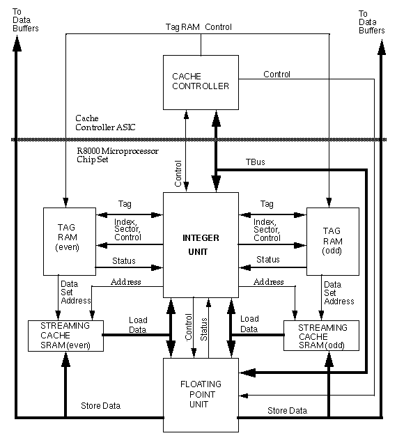
There are 7 basic parts to the system. Each is explained in more
detail in the following pages:
1) R8000 Microprocessor
2) R8010 Floating Point Unit
3) Tag RAM (even addresses)
4) Tag RAM (odd addresses)
5) Streaming Cache SRAM (Even data)
6) Streaming Cache SRAM (Odd data)
7) Cache Controller
Both the R8000 Microprocessor and the R8010 Floating Point Unit have
multiple execution units, allowing execution of 4 instuctions per clock;
two load/store instructions and two register to register or floating
point execute instructions. Separate integer and floating point units
maximize floating point throughput and allow for simultaneous execution
of integer and floating point instructions. The floating point unit
contains two pipelines, each of which can perform a double precision
multiply-add every cycle. Two identical tag RAM's store address
information for the even and odd data banks of the interleaved streaming
cache. The R8000 Microprocessor and R8010 Floating Point Unit interface
only to the streaming cache. Updates to the tag RAM's as well as all
transactions requiring interface to main system memory are handled by
the cache controller. Separate load and store data busses on the
floating point unit eliminate bus turnaround time and allow both loads
and stores to second level cache to execute simultaneously. Multiple tag
RAM's provide an interleaved caching scheme, allowing access times to
the cache to be hidden and providing two 64 bit operands to the R8010
FPU every clock.. A separate dirty bit RAM within each Tag RAM allows
for updating of the dirty bit status for one cycle at the same time as a
Tag RAM access for another cycle.
A set of compound multiply-add instructions has been added, taking
advantage of the fact that the majority of floating point computations
use the chained multiply-add paradigm. The operator for the multiply-add
instructions is not defined by the IEEE and does not perform
intermediate rounding. Eliminating the intermediate rounding step allows
for a lower inherent latency and has higher precision and higher
performance than an operator which performs intermediate rounding.
A register + register addressing mode for floating point loads and
stores has been added which eliminates the extra integer add required in
many array accesses. Register + register addressing for integer memory
operations is not supported.
A set of four conditional move operators allows IF statements to be
represented without branches. `THEN' and `ELSE' clauses are computed
unconditionally and the results placed in a temporary register.
Conditional move operators then transfer the temporary results to their
true register.
To allow the compiler flexibility in scheduling conditional moves and
their related comparisons, the Condition Code register has been expanded
to 8 bits.
Figure
1-1 shows a block diagram of the R8000 Microprocessor Chip Set. The
diagram is divided into two sections seperated by the thick dotted line.
All components below the thick dotted line constitute the R8000
Microprocessor Chip Set. Those components above the dotted line, the
Cache Controller and the Data Buffer Chips, are not part of the R8000
Microprocessor Chip Set. Consequently the Cache Controller is discussed
only in terms of functionality required. Package characteristics and
external pinout information are not discussed in this document. Refer to
section 3.0 for more information on the responsibilities of the Cache
Controller.
Figure 1-1: R8000 Microprocessor Chip Set Block Diagram
This section provides a more indepth look at the seven component
parts of the R8000 Microprocessor Chip Set. To provide the user with
maximum flexibility in system design, the cache controller was not
included as part of the R8000 Microprocessor. The Cache Controller is
also not offered as part of the chip set and is discussed only in terms
of functionality required.
The R8000 CPU is a 591 pin device and is the main computing component
of the system. The high pin count is a result of the numerous dedicated
busses provided by the R8000 CPU. This dedicated bussing scheme helps to
take full advantage of the multiple execution units within the R8000
CPU, allowing each unit to run independently of the other, alleviating
not only the need for multiplexing data and address, but also allowing
loads and stores to the streaming cache to occur simultaneously.
The R8000 CPU contains four caches and has dedicated interfaces to
all components in the system. The R8000 CPU performs address generation
and provides address information for interfacing to the streaming cache
via separate and dedicated address busses for the even and odd banks.
Instruction and data interface to the R8010 Floating Point Unit is via a
dedicated 80 bit TBus, and addresses to the tag RAM's are provided via
separate and dedicated tag, index, and sector busses for both the even
and odd tag RAM's.
The R8000 CPU contains two arithmetic logic units (ALU) as well as
two address generation units, and yields a maximum of 4 instructions per
cycle. The on-chip 16 KByte Data cache is dual ported and contains
separate address and 64 bit data busses for each port. This allows
multiple accesses to the cache to occur simultaneously. The 16 KByte
instruction cache is 128 bits wide and single ported. Both caches are
virtually indexed. The instruction cache is virtually tagged,
alleviating the need for address translation on I-cache accesses. The
data cache is physically tagged to maintain coherency with second level
cache. Each 32 byte line in the I-cache contains a specific address
space identifier (ASID). This value is assigned by the operating system
and is process specific. There are at least two specific ASID values per
process, one for the instruction cache, one for the TLB. The ASID helps
to differentiate between multiple processes within the same cache and
helps to reduce I-cache flushing by allowing the operating system to
invalidate only those lines whose process is no longer valid. The
operating system can also flush the I-cache when all 256 ASID values
have been used.
In addition to the data and instruction caches, the R8000 CPU also
contains Branch and Translation Lookaside Buffer (TLB) caches. The
Branch cache is accessed along with the instruction cache and is used to
predict and modify the program counter on branch or jump instructions.
The Branch Cache is a 15 bit field concatenated to each aligned 128 bit
quadword of the I-cache. The Branch Cache implements a simple branch
prediction mechanism which branches depending on the state of the
predict bit associated with each Branch Cache entry.
The TLB cache is used to convert virtual addresses to physical
addresses. A single TLB services both the data and instruction caches.
The instruction cache only requires address translation on a miss.
Similar to the instruction cache, each entry of the TLB also contains an
ASID. However, this value is different from that contained in the
I-cache. Having separate ASID values for each cache allows separate
flushing of the Instruction and TLB caches. Below is a list of features
of the four caches.
- 16 KBytes
- Virtually indexed
- Virtually tagged
- Direct mapped, no hashing
- Single ported, 128 bit path
- Fetches 4 instructions (128 bits) per cycle
- 32 Byte line size
- No parity
- 11 cycle miss penalty to streaming cache
- No coherency maintained with streaming cache
- Separate ASID values for I-cache tags
- Data Cache;
- 16 KBytes
- Virtually indexed
- Physically tagged
- Direct mapped, no hashing
- Dual ported, 64 bit data paths
- Two loads or one load and one store per cycle
- 32 Byte line size
- No parity
- 8 cycle miss penalty to streaming cache
- Coherency maintained with the streaming cache
- Write through with allocate protocol
- Separate ASID for D-cache tags
- Branch Cache;
- 1K Entries, one entry per 4 instr.
- Virtually indexed in parallel with Instruction cache
- Direct mapped, no hashing
- 3 cycle miss penalty
- TLB Cache;
- Dual ported, 2 translations/clock
- 3-way set associative,
- 384 entries total (128 X 3 way)
- Implements random replacement algorithm
- Supports 4K,8K,16K,64K,1M,4M,16M page sizes
- Maps one virtual to one physical page Indexed by low-order 7 bits of virtual address
- Index is hashed by Exclusive-OR of low order 7 bits of TLB cache ASID.
- Software Refilled
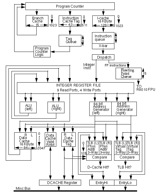
Figure 1-2: R8000 Microprocessor Block Diagram
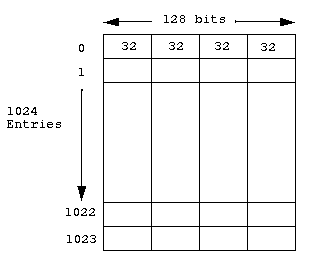
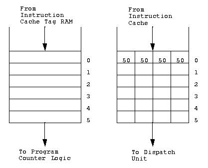
The instruction cache is 16 KBytes in size and is a direct-mapped
architecture arranged as 1024 entries by 128 bits. Each entry contains
four 32 bit instructions. Each access to the I-cache results in the
fetching of four instructions. The I-cache is virtually indexed and
virtually tagged, hence coherency between the I-cache and the physically
tagged Data Cache is not maintined. Figure
1-3 shows the organization of the instruction cache.
Figure 1-3: Instruction Cache Organization
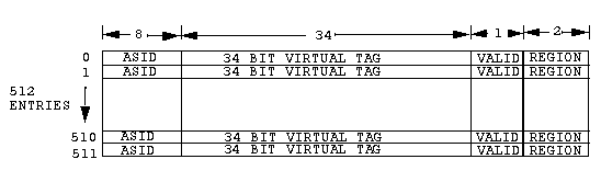
The I-cache line size is 32 bytes . There is one tag entry per
I-cache line. Each entry in the I-cache tag RAM consists of a 34 bit
tag, an 8 bit address space identifier (ASID), and a tag valid bit. The
ASID differentiates between processes and allows tag addresses from
different processes to reside in the I-cache tag at the same time.
The valid bit in the I-cache tag RAM defines whether the tag
information is valid. If the address tag compare is valid but the valid
bit for that entry is not set, an I-cache miss occurs. The valid bit is
used on I-cache misses to validate I-cache entries as the instructions
are written into the I-cache. The Region bits contain the values of bits
63:62 of the address bus and define one of the four addressing mode the
procesor is operating in. Figure
1-4 shows a block diagram of the instruction cache tag RAM.
Figure 1-4: Instruction Cache Tag RAM
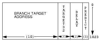
The Branch Cache works in conjunction with the instruction cache and
implements a simple branch prediction mechanism. The Branch Cache has
1024 entries, one entry for each 128 bit quadword in the instruction
cache. The total width of the Branch cache is 15 bits, 10 of which are
used to allow branching to any of the 1024 entries in the instruction
cache.
The branch cache does not detect the presence of branches in a given
I-cache line. Each branch cache entry has a predict bit associated with
it. If the predict bit is on, the corresponding 10 bit branch target
address is jammed into the program counter. The I-cache vectors to a new
index location and resumes the fetching of instructions. Whether or not
the branch prediction was correct is not known until 3 cycles later when
the branch instruction is actually executed. If the prediction is
correct, all of the I-cache entries in the pipeline following the branch
instruction will be correct and no cycles are lost. If the prediction
was incorrect, the pipeline is flushed. The new branch target address is
calculated and three cycles later instruction execution resumes.
The two bit DELAY field associated with each branch cache entry
encodes which of the four instructions in the I-cache entry contained
the branch instruction.
Since the compiler is not required to begin instruction execution on
a 128 bit boundary, the two bit TARGET32 field is encoded to indicate
where in the quadword the instruction execution began.There is one
TARGET32 field per branch cache entry. Figure
1-5 shows a diagram of the branch cache organization.
Figure 1-5: Branch Cache
Both the I-cache and the I-cache tag RAM have queues which act as
temporary storage for instructions waiting to be executed. Each queue is
six-deep. When instructions are fetched from the I-cache they undergo
predecoding before being placed in the queue. The purpose of predecoding
is to reduce instruction processing time in the decode stage of the
pipeline. Eighteen additional characterization bits are added to each
original 32 bit instruction.These bits are used for two cycles,
afterwhich most of the bits are no longer needed. By the time the
instructions reach the floating point queue they are 37 bits wide as
five bits of the original 18 additional bits will be used by the R8010
FPU. Predecoding accomplishes three things:
1) Consistent alignment of the 5-bit destination field.
2) Instruction Category encoding.
3) Addition of timing critical bits.
Figure
1-6 shows a block diagram of the instruction and tag queues.
Figure 1-6: Instruction and Instruction Tag Queues
The X-BAR determines which of the four instructions to send depending
on the resources available from cycle to cycle. This process is called
Resource Modeling. The idea behind resource modeling is that
instructions are not dispatched until there is sufficient resources
available for them to complete. The X-bar monitors the status of each
execution unit as well as determines interdependencies between any of
the four instructions in a given line.
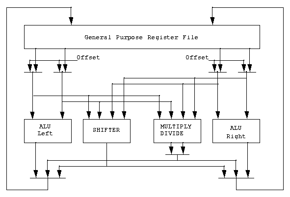
The integer register file in figure
1-1 consists of 9 read ports and 4 write ports. Four of the read
ports are dedicated to ALU usage. Four others are used for address
generation on integer or floating point memory operations. The ninth
read port is used for data cache stores and to implement certain load
alignment instructions. On D-cache stores the existence of the ninth
port reduces the amount of sharing that would normally be required by
those port(s) normally dedicated to address generation on memory
operations.
The Arithmetic Logic Unit (ALU) consists of two 64 bit arithmetic
units, one shifter, and one Multiply/Divide unit. The results of the
operations are written back to the register file. All arithmetic
operations occur in the execution stage (E-stage). Figure
1-7 shows a block diagram of the ALU.
Figure 1-7: Arithmetic Logic Units
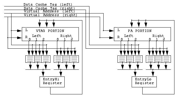
The Translation Lookaside Buffer (TLB) is dual ported and is
physically split into two halves. Each half contains 128 entries and is
3-way set associative, yielding a total of 384 entries each. One half
contains the virtual tags (VTAGS), the other the actual physical address
(PA) corresponsing to each virtual tag .
TLB, Data Cache, and Data Cache Tag RAM lookups are performed in the
execution stage (E-stage) of the pipeline. The VTAG portion of the TLB
is used to determine whether a certain range of addresses resides in the
PA portion. If it is determined that the translation for the virtual
address resides in the TLB, the contents of the PA portion is compared
to that in the D-cache tag RAM, resulting in either a hit or a miss to
the D-cache. Either a TLB or a D-cache miss initiates an external memory
cycle. Figure
1-8 shows a block diagram of the Translation Lookaside Buffer.
Figure 1-8: Translation Lookaside Buffer
The data cache is 16 KBytes organized as 2048 entries X 64 bits and
is dual-ported. Line size is 32 bytes. Two separate address and data
busses allow either two loads, or one store and one load to occur
simultaneously. The D-cache is virtually indexed and physically tagged
and implements a write-through protocol. All writes to the D-cache are
also written out to second level cache. Since only one store cycle can
occur at a time, the D-cache has one store aligner in the write path
between the register file and the D-cache. There are two load aligners
in the read path. These aligners assure that, if the requested data is
less than 64 bits, that data, regardless of where it is in the 64 bit
doubleword, will be shifted to the proper place within the doubleword
before being written to the register file. The store aligner performs
the opposite function by shifting the requested data of the register to
the desired location in the 64 bit doubleword before writing it to the
D-cache.
One Byte is the smallest writeable quantity to the D-cache, meaning
that the R8000 CPU can write any or all bytes within a given 64 bit
doubleword. Read cycles have the same resolution. Although the D-cache
write size is variable, the streaming cache is not and requires a
minimum of 32 bits on every write cycle. Therefore even though the R8000
CPU may write less than 64 bits to the D-cache, it must assure that a
minimum of 32 bits of the given doubleword are placed on the bus when
the write to the streaming cache is initiated.
The data cache tag RAM contains 512 entries, one entry per 32 byte
D-cache line. Each tag entry is 28 bits wide.
When the RAM is indexed, the corresponding physical tag is compared
to the translated address from the TLB. On loads the tag RAM is accessed
at the same time as the D-cache. There is no time lost waiting for the
result of the TLB lookup. By the time the status of the TLB lookup is
determined the D-cache has been indexed and the data read out. If it is
determined that the requested address is in the cache, the data is
written to the register file in the same clock and the cycle is
completed. If the requested address is not in the cache, the buffers
which allow the data to write the register file are simply not enabled.
A D-cache miss occurs and a memory cycle to second level cache is
initiated. Simultaneous access of the D-cache and the tag RAM allows for
single clock reads when there is a D-cache hit.
D-cache stores are done the same way as loads. The TLB lookup and the
accompanying store to the D-cache occur in the same clock. If either the
virtual or physical address compare did not match, resulting in either a
TLB or D-Cache miss, the store location in the D-cache is invalidated in
the next clock by turning off the valid bit in the D-cache Valid RAM
location corresponding to the store.
The data cache Valid RAM is 4 bits wide and contains 1024 entries.
Each entry represents a 32 bit value, hence there are two valid bits per
64 bit doubleword. Each index to the valid RAM corresponds to the status
of two 64 bit Data cache words. There are two reasons for a separate
valid RAM with individual bits:
The first reason is to alleviate invalidating entire lines of the
cache when floating point data is found. Sometimes integer and floating
point data reside in the same data cache (D-cache) line. Floating point
loads and stores interface directly to the streaming cache and do not
usually affect the contents of the R8000 CPU data cache. However, the
data cache of the R8000 CPU must be kept coherent with the streaming
cache. Therefore, if a FP store is done to a given location in the
streaming cache which also resides in the D-cache, the D-cache entry
must be invalidated. By having individual valid bits for each 32 bit
word in the data cache, the mixing of floating point and integer data in
a given D-cache line is better accomodated. This way if an integer load
is done to that same location a D-cache miss occurs, forcing the R8000
CPU to fetch the data from the streaming cache.
The second reason for having a separate valid RAM is to be able to
easily invalidate the data for integer stores which miss in the D-cache.
In the R8000 CPU data is stored to the D-cache in the same cycle that
the TLB and D-cache hit/miss status is determined. This is done so that
the store data does not have to wait for the result of the lookup before
it is written to the D-cache. If a store miss occurs the data is
invalidated in the following cycle by turning the valid bit off for that
D-cache entry.
Valid bits are checked on both loads and stores. Because the D-cache
contains only data it does not know whether a given location contains
integer or FP data, only whether the entry is valid or not valid.
Figure
1-9 shows the organization of the data cache.
Figure 1-9: Data Cache, Data Cache Tag, Data Cache Valid RAM
Organization
The R8010 Floating Point Unit (FPU) is a 591 pin device which
performs all floating point functions for the R8000 Microprocessor Chip
Set. The R8010 FPU has two execution units, allowing two arithmetic and
two Floating Point memory operations to be executed every clock. The
Floating Point Register File contains 8 read ports and 4 write ports.
Large load and store data queues, each 32 entries deep, allow for a
pipelined interface between the R8000 CPU and the R8010 FPU,
streamlining the flow of data and minimizing wait time. With a target
frequency of 75 MHz, the Floating Point Unit offers a peak performance
of 300 MFLOPS.
The R8010 FPU has no on-chip cache and uses the streaming cache,
which is the second level cache of the R8000 CPU, as its memory.
Dedicated load and store data busses to both the even and odd banks of
streaming cache allow a read or write operation to be performed every
clock. An 80 bit TBus interface forms the control bus for the R8010 FPU
and allows the R8010 FPU to interface to both the R8000 CPU and the
Cache Controller (CC). Normally the R8010 FPU is controlled by the R8000
CPU. Dispatching of instructions, floating point loads and stores to the
streaming cache, integer stores to the streaming cache, etc. are all
under control of the R8000 CPU. Cycles which miss in the streaming cache
and require interface to the main memory are handled by the Cache
Controller. For these cycles the R8010 FPU is used only to transfer data
from the load data bus to the store data bus.
Floating point instructions are received from the R8000
Microprocessor through the TBus. The instructions are executed and the
result written back to the FP register file. Floating Point data is
retrieved from the streaming cache on the load data pins and then placed
in the Load Data Queue. For store operations data from the result is
placed in the store data queue. As soon as the corresponding address
information from the Tag RAM is made available, the data is written out
to the streaming cache. In addition to floating point operations, the
R8010 FPU is also used during integer stores to the streaming cache,
handled by the R8000 CPU, as well as stores to main memory, handled by
the CC.
A set of compound multiply-add instructions has been added, taking
advantage of the fact that the majority of floating point computations
use the chained multiply-add paradigm. The operator for the multiply-add
instructions is not defined by the IEEE and does not perform
intermediate rounding. Eliminating the intermediate rounding step allows
for a lower inherent latency and has higher precision and higher
performance than an operator which performs intermediate rounding.
Figure
1-10 shows a block diagram of the floating point unit.
Figure 1-10: R8010 FPU Block Diagram
The R8010 FPU performs three basic types of arithmetic operations
denoted as Short, Regular, and Long. Each operation has some number of
clocks associated with its staging as well as latency. Staging defines
how long the unit is busy. Latency defines the amount of delay clocks
before the results are available. Each execution unit is fully pipelined
and can begin a new operation on every clock.
Short operations have a one clock staging and one clock latency and
include such move operations as MOV, MOVC, MOVZ, MOVN, NEG, ABS, and C.
Except for Compares (C), short operations can be issued while long
operations are executing. Compare instructions target the condition code
field of the ControlStatus Register.
Regular operations have one cycle staging and four cycle latency.
These include add, subtract, and multiply operations such as ADD, SUB,
MUL, MADD, MSUB, CONVERT. Regular operations can require either 1, 2, or
3 source operands from the FP register file. These operands are read
from the FPR. Each of the operations takes four cycles to complete. On
the next clock the result is written back to the FPR. On-chip bypass
logic allows the results of regular operations to be written to the FPR
and at the same time back into the executions units. When the result of
one operation is required for the operation immediately following, the
bypass logic allows the result to be used in the next clock instead of
having to write to the FPR and then read the information back out in the
next clock.
Long opertaions have variable latency and staging times and include
such operations as DIV, SQRT, RECIP, RSQRT. These times are shown in
table 1 below.
Operation           Latency               Staging

DIV.S                 14                    11

DIV.D                 20                    17

SQRT.S                14                    11

SQRT.D                23                    20

RECIP.S               8                     5

RECIP.D               14                    11

RECIPSQRT.S           8                     5

RECIPSQRT.D           17                    14

Table 1-1
Instructions are dispatched by the R8000 CPU to the R8010 FPU through
the TBus. There are four basic types is transmissions which are
differentiated by encoding the uppermost two bits of the TBus:
Normal - A normal dispatch contains two FP arithmetic operations,
each 28 bits wide, and two FP memory operations, each 9 bits wide. There
are roughly 30 FP arithmetic operations which can be dispatched by the
R8000 CPU. The 28 bit TBus format for arithmetic operations is different
for each operation. For FP memory operations, the 9 bit value contains
Floating Point Register destination as well as data alignment
information. Each of the four potential instructions contains a valid
bit associated with it. These four valid bits form the upper bits of the
TBus. Setting this bit indicates to the R8010 FPU that a given
instruction is valid and should be executed.
Move From - MoveFrom is similar in format to Normal mode except that
the FP memory operation normally on TBus bits 73:64 is substituted with
a move specifier. This operation moves data from a FP register to a
general purpose register (GPR) in the R8000 CPU and is the only time
which the R8010 FPU drives the TBus.
IntStore - The IntStore operation supports integer stores to the
streaming cache. As shown in figure
1-1, there is no direct path for integer stores from the R8000 CPU
to the streaming cache. Instead they are transmitted across the TBus and
out onto the store data pins of the R8010 FPU. In IntStore mode the TBus
contains the 64 bit integer data along with some store alignment
information.
MoveTo - This operations moves data from a General Purpose Register
(GPR) in the R8000 CPU to a Floating Point Register. The MoveTo format
is similar to the IntStore format except that instead of store alignment
information, TBus bits 73:65 contain the FPR destination. The 64 data is
transmitted on TBus pins 63:0.
Table 2 shows the TBus format for each of the four basic
transmissions.
TBus Bits  79 78    77      76      75      74    73  65    64 63 56    55  28         0

Normal      1 0     Vma     Vmb     Vfa    Vfb    MSpecA    MS pec B    FpOP-A    FpOP-B

MoveFrom    0 1     Vmf     Vmb     Vfa    Vfb    MfSpec    MS pec B    FpOP-A    FpOP-B

IntStore    0 0     1       ---     ---    ---    IStSpec     -         Data

MoveTo      1 1     1       ---     ---    ---    MtSpec      -         Data

Table 1-2
Two identical tag RAM's are required in the R8000 Microprocessor Chip
Set in order to support the interleaved architecture of the second level
streaming cache. Both RAM's contain the same information. One is used
for the even bank, the other for the odd bank. The two banks are
differentiated by the state of address bit A3. If this bit is low the
access is to the even bank. A high on this pin enables the odd bank. Figure
1-11 shows a block diagram of the tag RAM.
Figure 1-11: Tag RAM Block Diagram
The Tag RAM is 4-way set associative and is organized as 8192 entries
X 128 bits. Each entry contains 32 bits of information for each of the
four ways, hence the 128 bit width. The 32 bits of each way is further
broken down into a 20 bit tag address, 4 virtual synonym bits, and 8
state bits. Figure
1-12 shows the Tag RAM bit assignments.
Figure 1-12: Tag RAM Bit Assignments
There are three basic cycles performed on the tag RAM:
1) Lookups
2) Reads
3) Writes
Lookups are performed by the R8000 CPU and are done when the R8000
CPU wants to either read or write second level cache. The R8000 CPU
supplies dedicated tag, index, sector, and control lines to each tag
RAM. In a set associative cache implementation the R8000 CPU does not
know which of the sets of a given address the data is contained. The tag
RAM compare supplies this information in the form of a 2 bit encoded
value. This value forms the two upper bits of the streaming cache
address and determines which of the sets the data resides. The R8000 CPU
does not read or write the tag RAM directly except for the dirty bit. If
a write lookup gets a hit to the Tag RAM, indicating that the data
exists in the streaming cache, the data is written out to the cache and
the dirty bit is set on the next clock. If the line is in the exclusive
state and it is unmodified (clean), setting of the dirty bit changes the
state of the line from exlusive clean to exclusive dirty. If the line is
already in the modified state (dirty) the dirty line must be written out
to main memory before the write can be completed.
Read cycles are initiated by the Cache Controller (CC) and inform the
CC of the status of a given entry. Information exchange is through the
TBus. The CC supplies the 2 bit set address along with the proper
control signals. The information is read from the read logic block
internal to the tag RAM in figure
1-11.
Write cycles are also performed by the Cache Controller and are done
when the CC wants to modify an entry. Refer to figure
1-11. On write cycles the tag, index, and sector information are
generated by the CC and transferred to the R8000 CPU on the TBus. The
R8000 CPU plays no part in a write cycle other than to pass the
information from the TBus onto the appropriate dedicated busses of the
even and odd Tag RAM's.
Note that the 20 bit tag field connects to both the address write and
V.S. write blocks. Hence the tag pins contain different information
based on whether the CC is writing the address, or the state and V.S.
bits. Only one of these writes can be executed at a time.
The Dirty Bit RAM in figure
1-11 is organized as 8192 entries X 16 bits. The number of entries
is the same as the tag RAM and is indexed in the clock after the Tag RAM
access. The purpose of a separate Dirty Bit RAM is to allow the status
of a given line to be changed during a Tag RAM access. Therefore if
there is a write to the streaming cache and the dirty bit status for
that write must be updated, the dirty bit can be set on the next clock,
even though the Tag RAM has already started an access for the next
cycle. The 2 bit state field in the tag RAM identifies the status of the
entry; either invalid, shared, or exclusive. The exclusive line can
either be clean or dirty. The Dirty Bit RAM maintains this information.
In a sectored cache implementation there is one dirty bit for each
sector. Therefore the dirty bits are not always the same for both the
even and odd Tag RAM's. The address, state, and virtual synonym
information is always the same for both Tag RAM's, but the dirty bit
information can be different.
The streaming cache data RAM's have separate load and store data
busses. Although only one cycle can be performed by the data RAM's at a
time, both read and write data can be on their respective busses at the
same time. Having separate busses eliminates any bus turnaround time,
which occurrs on back to back read followed by write cycles, and allows
read and write data to be pipelined to the RAM, effectively allowing the
RAM to perform a read or write operation every clock.
The total memory size is split between the even and odd banks. Each
bank contains 2 MBytes and has a dedicated Tag RAM, allowing accesses to
the banks to operate simultaneously and independently of one another.
The RAM is buffered by input and output data registers. If the RAM is
performing a read and write data appears on the input bus, the data is
placed in the register. Self-timed write logic allows the RAM to write
the data as soon as the RAM finishes the previous read cycle.
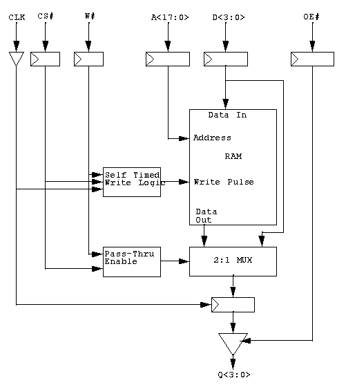
The 4 MByte streaming cache is implemented using 256 K X 4 Data
RAM's. Each individual data RAM is be 256K x 4 bits wide and has
separate read and write busses. Figure
1-13 shows a block diagram of the 256K X 4 Data RAM.
Figure 1-13: Data Ram Architecture Block Diagram
The Data RAM's must support four types of cycles which are decoded by
the CS# and WE# bits:
1) /CS * /W = Write and Pass through
2) /CS * W = Read
3) CS * /W = Pass through
4) CS * W = Don't care
The Pass through mode allows data on the input (write) bus to be
passed onto the output (read) data pins through a multiplexor. All write
cycles can also be pass-through. Data which is written to the RAM is
also sent to the output mux. The mux is controlled by the CS# and W#
pins. Read cycles are standard in that the RAM is accessed and data
placed on the outputs. Maximum clock to out time is 7 nS. The RAM can
also be operated in pass through mode where data is passed from the
inputs to the outputs without being written to the RAM. The Don't care
mode causes the output buffers to tri-state. Parity is handled in
sixteen bit quantities. Parity timing is identical to data timing.
The cache memory system architecture consists of sets, lines, and
sectors. In order to help the reader understand the cache memory
architecture, the following example discusses a 4 MByte SIM module
implementation in a 4-way set associative configuration with 128 bytes
per sector and four sectors per line.
There are nine devices per SIM module, 8 data RAM's and 1 parity RAM,
which yield 1 MByte. A minimum of two SIM modules are required to
interface to the 64 bit external bus of the R8000 Microprocessor.
The 4-way set associative cache consists of 2048 lines. Each line
consists of four sectors. Each sector contains sixteen 64-bit words
divided as 8 words per bank. So each line contains 512 bytes, 256 bytes
per bank. Since there are four sectors per line each sector contains 128
bytes. Refer to figure
1-14.
Figure 1-14: Four MByte Streaming Cache Organization
The Data Set Address (DATSA) pins form the upper two bits of address
for the cache and are used to differentiate between the four banks.
Addressing the entire 4 MByte cache requires 22 address bits. The 256K
RAM uses 18 of these bits. Accesses to the second level cache can either
be in 32 or 64 bits quantities. Each 32 bit SIM module in the 4 MByte
example has a dedicated write enable, allowing only 32 bits of the word
to be written by the R8000 CPU. The address breakdown is as follows:
A<19:9> 11 bits - Decodes one of 2048 lines per set.
A<8:7> 2 bits - Decodes one of four sectors per line.
A<6:4> 3 bits - Decodes one of eight 64 bit words per sector.
A<3> 1 bit - Determines which bank is accessed.
A<2:0> 3 bits - Decodes a given byte within a 64 bit doubleword.
-------
22 address bits total = 4 MByte cache.
This section is intended to be an overview of the responsibilities of
the cache controller and is not intended to be used as a design guide.
The processor to cache interface is far more complex than what is
described here. A more in-depth discussion of the processor/cache
interface is available in the R8000 User's Manual.
The R8000 Microprocessor Chip Set has large first and second level
caches which minimize the need for interfacing to external main memory.
Main memory is typically slow and when accessed frequently can degrade
the overall performance of the processor. To maximize performance, the
R8000 Microprocessor interfaces only to the 16 KByte on-chip cache and
the streaming cache. The Floating Point Unit interfaces only to the
streaming cache. Neither device inititates cycles or interfaces directly
to the main memory. However, there are times when interfacing to the
external main memory is necessary.
The interface to external main memory is the responsibility of the
Cache Controller. The Cache Controller (CC) performs the following
duties:
1) Fetching data from main memory on a streaming cache miss.
2) The write-back of dirty data from the streaming cache to main
memory.
3) Modification of streaming cache tags, state, and virtual synonym
information in the Tag RAM.
4) Invalidation of the Data cache when the streaming cache is
modified.
5) All coherence issues between streaming caches in a multiprocessor
environment.
6) Filtering of coherence activity so that the R8000 Microprocessor
is protected from unnecessary interruptions.
7) Checking of the store address queue so that it appears to the
system as an extension of the streaming cache.
8) Local registers for interrupt prioritizing and management.
The Cache Controller is also required to handle booting from a ROM
device and transferrence of ROM data into the streaming cache, control
signal generation for the data buffers which interface to external main
memory, and maintaining a bus copy in a third Tag RAM. The third Tag RAM
is recommended and is used to monitor snooping activity on the bus. The
two Tag RAM's which interface to the two banks of the streaming cache
require all of their bandwidth to maintain a single cycle access rate.
Use of the third Tag RAM eliminates these two Tag RAM's from having to
monitor bus activity. This enhances performance and reduces Tag RAM
overhead.
On a streaming cache miss, the R8000 CPU transfers control of the bus
to the CC. When control of the bus is transferred is determined by the
CC state machine which has 5 full states and 4 transition states. While
the CC is in control of the bus it must:
1) Update the streaming cache data.
2) Update the Tag RAM's.
3) Update the Store Address Queue.
4) Update the Data Cache Valid bits.
5) Update the Interrupt pending flag.
6) Update the Sequential Update flag.
It is only after these duties are completed that control of the bus
is returned to the R8000 CPU.
On R8000 CPU misses to the streaming cache the R8000 CPU informs the
CC that the requested data was not available. Control of the bus is then
transferred to the CC. Since neither the R8000 CPU or the R8010 FPU
communicate directly with external main memory, it is the responsiblilty
of the CC to fetch the requested data from main memory and place it in
the streaming cache. Once the cycle is completed the CC relinquishes
control of the bus back to the R8000 CPU. The R8000 CPU then fetches the
requested data from the streaming cache and execution resumes.
In addition to streaming cache misses, the CC is responsible for
monitoring the cache coherency attributes of each line in the cache.
This is done via the 16 bit Dirty Bit RAM portion of the Tag RAM as well
as the Tag RAM itself. If the state of the line in the cache changes,
the state information in the Tag RAM must also be updated to reflect the
change. If the state of the line remains the same and only the modified
status changes, only the dirty bit is accessed. State information
remains the same. Changing the state information is the responsibility
of the CC. Updating of the dirty bit RAM is done by the R8000 CPU.
Since the first level cache is write-through, all writes by the R8000
CPU to the first level Data cache are also written out to the streaming
cache. If a write is executed to a line which has already been modified,
the CC will tell the R8000 CPU to halt the cycle and take control of the
bus. The modified data is then written out to main memory and control of
the bus given back to the R8000 CPU.
The Cache Controller is responsible for monitoring and updating of
the Tag RAM. The R8000 CPU performs only Look-up cycles to the Tag RAM.
These are done when the R8000 CPU wishes to read or write the streaming
cache and desires to know which set of the streaming cache the data
resides in. Read and write cycles to the Tag RAM are performed by the
CC.
The CC can write either Tag information, or state and virtual synonym
information to the Tag RAM in a given cycle. Refer to figure
1-11. The Tag address is multiplexed with either tag or state and
virtual synonym information. When the tag address is updated, the 20 bit
tag bus contains all address bits. When the state and virtual synonym
information is updated, the tag bus conforms to a specific bit
orientation. The bit orientation changes for state and virtual synonym
read cycles. Whenever there is a streaming cache miss, or when a line of
the streaming cache is to be written out to main memory, the Tag RAM
information must be updated to reflect this change. The CC must supply
all necessary control signals to the Tag RAM.
During normal operation the TBus is used for transferring information
between the R8000 CPU and the R8010 FPU. During this time the CC
interfaces to the main memory backplane interface bus, as well as
monitors the third Tag RAM and the hit/miss status of R8000 CPU to
streaming cache cycles. When a streaming cache miss or a coherence
operation on the bus occurs, the TBus is used to transfer information
between the R8000 CPU and the CC. The bit orientation and definition of
the Tbus changes depending on whether the R8000 CPU or the CC is driving
the TBus. The TBus for the system is 80 bits wide. However, the
uppermost 8 bits are dedicated between the R8000 CPU and the R8010 FPU.
The R8000 CPU to CC TBus is 72 bits.
When the R8000 CPU is in control of the TBus, the orientation and
definition of the TBus is as follows:
The Command field is a four bit field which encodes the type
of memory access the R8000 CPU was doing which caused the transfer. Also
included in the command field are the Cacheable and Non-cacheable
coherence attributes of each access type.
The Size field is an encoded three bit value which indicates
the size of the operation, one through eight bytes, for non-cacheable
operations.
The Coherence Protocol field is a three bit field used to
indicate the coherence atributes in the page table entry for the access.
It is used to determine whether the access is cacheable, and what type
of protocol to follow in filling the streaming cache.
The No Match field is a two bit field which reflects the
status of the MATCH pin which was returned to the R8000 CPU by the Tag
RAM. The R8000 CPU samples the various control signals from the Tag RAM
and encodes the status of the Tag RAM lookup in the No-Match field of
the TBus. The No Match field also contains the status of whether the
virtual synonym returned from the Tag RAM matched the virtual address
bits from the original address. The number of virtual synonym bits
actually checked depends on the size of the Data Cache. If the No-Match
field indicates both a Tag address match and a virtual synonym match,
the CC simply fetches and adds a sector to the existing line. If the
field indicates a Tag address match and a virtual synonym mis-match, the
CC removes the entire line, invalidates the corresponding entry in the
Data Cache, fetches the needed sector and places it in the streaming
cache (in the same set). If there is no Tag address match, indicating a
miss, the CC removes the entire line at a set which the CC chooses,
invalidates the Data Cache entry for athat line, fetches the needed
sector and places it in the streaming cache at that set.
The Set Address field is a two bit field which reflects the
status of the Tag RAM lookup and distinguishes which of the four sets in
the Tag RAM the address compared.
The State field is a two bit field which indicates the
coherency status for the given access; Invalid, Shared, or Exclusive.
The Virtual Synonym field is a four bit field which represents
the status of virtual address bits 15:12 of the access which caused the
operation.
The Physical Address is a 40 bit field and is used directly in
processing the operation.
When the CC is in control of the Tbus, the orientation and definition
of the Tbus bits is as follows:
The Function Field is a four bit field and is the only field
by which the CC changes the internal state of the R8000 CPU instead of
just the Tag RAM's or the streaming cache RAM's. There are a number of
different operations which can be performed based on the state of the
function field. The function field controls such operations as
invalidation of the first level Data Cache, instructing the R8000 CPU to
empty the floating point store address and store data queues by briefly
returning the TBus to the R8000 CPU for this operation, interrupt
status, and signal generation for reading the Tag RAM.
The Data RAM Write Enable field is a four bit field which
contains the write enables for the streaming cache. Assertion of each
write enable controls the write of a word (4 bytes).
The Data RAM External Set Address field is a two bit field
which encodes which of the four sets of the streaming cache the data is
to be written.
The Data RAM Address field is an 18 bit field containing
address bit 21:4 and forms the address for the streaming cache RAM's.
Address bits 3 and 2 determine which write enables are asserted on the
TBus. Address bits <1:0> are not generated by the CC as 32 bits is
the smallest writeable quantity.
The Tag RAM Address field is a 35 bit field used to read and
write the even and odd Tag RAM's address. The state and virtual synonym
information is also written using these bits. The size of the field is
large enough to support a 16 MByte streaming cache configuration.
The Virtual Synonym field is used to assure that the correct
location is invalidated during a data cache invalidation cycle. The
indesx to the data cache Tag RAM internal to the R8000 CPU is formed by
TBus bits <15:5>. The four bit virtual synonym field, TBus
<3:0> is concatenated with tag address bits <39:16> to form
the data cache address. The address is used for the data cache tag
comparison to determine whether the location to be invalidated resides
in the data cache. PRODUCT OVERVIEW
1.0 INTRODUCTION TO THE R8000 MICROPROCESSOR CHIP SET
1.0 INTRODUCTION TO THE R8000 MICROPROCESSOR CHIP SET
2.0 R8000 FUNCTIONAL UNITS
2.1 R8000 Microprocessor
- Instruction cache;
2.1.1 INSTRUCTION CACHE
2.1.2 INSTRUCTION CACHE TAG RAM
2.1.3 BRANCH CACHE
2.1.4 INSTRUCTION QUEUE
2.1.5 X-BAR
2.1.6 GENERAL PURPOSE REGISTER FILE
2.1.7 ARITHMETIC LOGIC UNIT
2.1.8 TRANSLATION LOOKASIDE BUFFER
2.1.9 DATA CACHE
2.1.10 DATA CACHE TAG RAM
2.1.11 DATA CACHE VALID RAM
2.2 R8010 FLOATING POINT UNIT
2.2.1 R8010 FPU OPERATIONS
2.2.2 TBUS INTERFACE
2.3 TAG RAM
2.3.1 TAG RAM ORGANIZATION
2.3.2 TAG RAM CYCLE TYPES
2.3.3 DIRTY BIT RAM
2.4 STREAMING CACHE DATA RAMS
2.4.1 DATA RAM ARCHITECTURE
2.4.2 CACHE MEMORY SYSTEM ARCHITECTURE
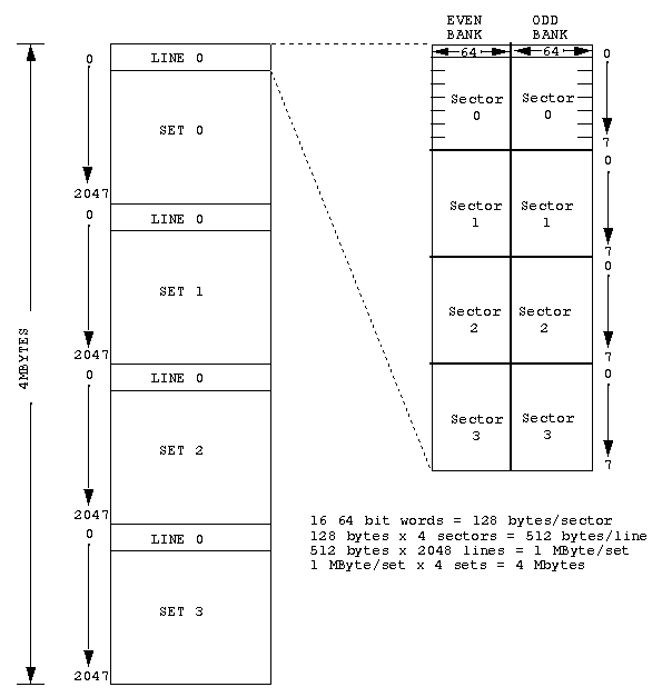
DATSA<1:0> 2 bits - Decodes one of four sets in the cache.
3.0 RESPONSIBILITIES OF THE CACHE CONTROLLER
3.1 CACHE CONTROLLER OVERVIEW
3.1.1 STREAMING CACHE DATA MANAGEMENT
3.1.2 TAG RAM MANAGEMENT
3.1.3 TBUS INTERFACE
3.1.3.1 R8000 CPU TO CC TBUS PROTOCOL
FIELD                 WIDTH     TBUS BITS
-----                 -----     ---------
Reserved               12        71:60
Command                4         59:56
Size                   3         55:53
Coherence Protocol     3         52:50
No Match               2         49:48
Set Address            2         47:46
State                  2         45:44
Virtual Synonym        4         43:40
Physical Address       40        39.0
3.1.3.2 CC TO R8000 CPU TBUS PROTOCOL
FIELD                    WIDTH     TBUS BITS
-----                    -----     ---------
Reserved                  4         71:68
Function                  4         67:64
Data RAM Write En.        4         63:60
Data RAM Ext. Set Adr.    2         59:58
Data RAM Addr<21:4>       18        57:40
Tag RAM Addr<39:5>        35        39:5
Reserved                  1         4
Virtual Synonym           4         3:0